

|
| MOQ: | 1 pair |
| Standard Packaging: | 4pcs/plastic plate, |
| Delivery Period: | Within 1-3 work days |
| Payment Method: | L/C, T/T, Western Union,Credit Card |
| Supply Capacity: | 10,000 pcs per month |
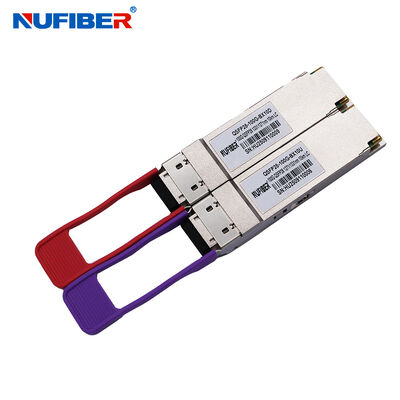
100Gb/s QSFP28 BIDI 10km DDM Transceiver
Descriptions
The 100G QSFP28 LR1 BIDI is designed for 10km optical communication applications. It is intended for the service with single mode fiber in 100Gb/s high speed data communications. The optical signals are multiplexed to a single-mode fiber through commercial standard LC connector.
Product Features
Applications
Ordering Information
| Part No. | Data Rate(optical) | Laser | Fiber Type | Distance | Optical Interface | Temp | DDMI | Latch Color |
| QSFP28-100G-BX20U | 106.25Gbps | Tx1271/Rx1331 | SMF | 20km | LC | 0~70C | Y | Purple |
| QSFP28-100G-BX20D | 106.25Gbps | Tx1331/Rx1271 | SMF | 20km | LC | 0~70C | Y | Red |
I. Absolute Maximum Ratings
| Parameter | Symbol | Min. | Typical | Max. | Unit | Notes |
| Storage Temperature | TS | -40 | - | +85 | °C | |
| Supply Voltage | VCC | -0.5 | - | +4.0 | V | |
| Operating Relative Humidity | RH | - | - | +85 | % |
II. Recommended Operating Conditions
| Parameter | Symbol | Min. | Typical | Max. | Unit | Notes |
| Operating Case Temperature | TC | 0 | - | +70 | °C | |
| Power Supply Voltage | VCC | 3.13 | 3.3 | 3.47 | V | |
| Transmission Distance | TD | - | - | 10 | km | Over SMF |
III. Optical and Characteristics
| Parameter | Symbol | Min. | Typical | Max. | Unit | Notes |
| Transmitter | ||||||
| Center Wavelength | CW | 1264.5 | 1271 | 1277.5 | nm | |
| 1324.5 | 1331 | 1337.5 | nm | |||
| Signaling Rate | SR | 53.125 | GBd | |||
| Frequency Offset | Foffset | -100 | 100 | ppm | ||
| Average Launch Power | PTX | -1.4 | - | 4.5 | dBm | 1 |
| Outer Optical Modulation Amplitude | OMA | 0.7 | - | 4.7 | dBm | 1 |
| Launch power in OMA minus TDECQ | OMA-TDECQ | -0.7 | - | - | dBm | ER≧4.5 dB |
| -0.6 | - | - | dBm | ER<4.5dB | ||
| Transmitter and dispersion eye closure for PAM4 (TDECQ) (max) | TDECQ | - | - | 3.4 | dBm | |
| Average Output Power (Laser Turn off) | Poff | - | - | -30 | dBm | |
| Side Mode Suppression Ratio | SMSR | 30 | - | - | dB | |
| Extinction Ratio | ER | 3.5 | - | - | dB | |
| RIN_OMA | RIN | - | - | -136 | dB/Hz | |
| Transmitter reflectance | Tref | - | - | -26 | dB | |
| Optical Return Loss Tolerance | ORLT | - | - | 15.6 | dB | |
| Receiver | ||||||
| Center Wavelength | CW | 1324.5 | 1331 | 1337.5 | nm | |
| 1264.5 | 1271 | 1277.5 | nm | |||
| Damage threshold | Pdamage | 5.5 | - | - | dBm | 2 |
| Average Rx Power | PRx | -7.7 | - | 4.5 | dBm | 3 |
| Receive power _OMAouter | POMA | - | - | 4.7 | dBm | |
|
Receiver sensitivity _OMAouter for TDECQ < 1.4 dB for 1.4 dB £ TDECQ £ 3.4 dB |
SEN _OMA | - | - |
-6.1 –7.5 + TDECQ |
dBm | 4 |
| Reflectance | Ref | - | - | -26 | dB | |
| Los Assert | LosA | -26 | - | dBm | ||
| Los De-Assert | LosDA | - | - | -10 | dBm | |
| Los Hysteresis | LosH | 0.5 | - | - | dB | |
| Stressed receiver sensitivity _OMAouter | SRS | - | - | -4.1 | dBm | 5 |
| Conditions of stressed receiver sensitivity teste : | ||||||
| Stressed eye closure for PAM4 (SECQ) | 3.4 | dB | 6 | |||
| SECQ-10*lgCeq | 3.4 | dB | 6 | |||
Notes:
IV. Electrical Characteristics
| Parameter | Symbol | Min. | Typical | Max. | Unit | Notes |
| Transmitter (Module Input) | ||||||
| Input Differential Impedance | Rin | - | 100 | - | Ohm | |
| Differential Data Input Amplitude | VIN,P-P | - | 900 | mVpp | ||
| Differential termination mismatch (max) | D-mismatch | - | - | 10 | % | |
| DC common-mode input voltage | -0.3 | - | 2.8 | V | ||
| Transition time(20%~80%) | Tr Tf | 10 | - | - | ps | |
| LPMode, Reset and ModSelL / Tx dis | VIL | -0.3 | - | 0.8 | V | |
| LPMode, Reset and ModSelL / Tx dis | VIH | 2.0 | - | VCC+0.3 | V | |
| Receiver (Module Output) | ||||||
| Output Differential Impedance | Rout | - | 100 | - | Ohm | |
| Differential Data Output Amplitude | VOUTP-P | - | - | 900 | mVpp | |
| Differential termination mismatch (max) | D-mismatch | - | - | 10 | % | |
| Transition time, 20% to 80% | Tr Tf | 12 | - | ps | ||
| ModPrsL and IntL/ Rx los | VOL | 0 | - | 0.4 | V | |
| ModPrsL and IntL/ Rx los | VOH | VCC-0.5 | - | VCC+0.3 | V | |
V. Digital Diagnostics
| Parameter | Range | Accuracy | Unit | Calibration |
| Temperature | 0 to 70 | ±3 | ºC | Internal |
| Voltage | 0 to Vcc | ±3% | V | Internal |
| Tx Bias Current | 0 to 100 | ±10% | mA | Internal |
| Tx Output Power | -1.4 to 4.5 | ±3 | dB | Internal |
| Rx Input Power | -7.7 to 4.5 | ±3 | dB | Internal |
VI. Communication Interface Timing Characteristics
| Parameter | Symbol | Min | Max | Unit | Calibration | Notes |
| Initialization time | t_init | 10 | s | Time from power on or hot plug until the module is fully functional. This time applies to Power Class 2 or higher modules when LPMode is pulled low by the host, and to all Power Class 1 modules. |
Room Temperature |
|
| LPMode Assert Time | ton_LPMode | 100 | ms | Time from when the host releases LPMode to high until module power consumption reaches Power Class 1. | ||
| Rx LOS Assert Time | ton_LOS | 100 | ms | Time from Rx optical signal loss to Rx LOS bit set to 1 and IntL pulled low by the module. | ||
| Tx Fault Assert Time | ton_Txfault | 200 | ms | Time from Tx Fault state to Tx Fault bit set to 1 and IntL pulled low by the module. | ||
| Tx Disable Deassert Time | toff_TxDis | 400 | ms | Time from Tx Disable bit cleared to 0 until optical output rises above 90% of nominal. | ||
| Tx Disable Assert Time | ton_TxDis | 100 | ms | Time from Tx Disable bit set to 1 until optical output falls below 10% of nominal. |
VII. Pin Diagram
![]()
VIII. Pin Definitions
| PIN | Logic | Symbol | Description |
Plug Seq. |
Notes |
| 1 | GND | Ground | 1 | 1 | |
| 2 | CML-I | Tx2n | Transmitter Inverted Data Input | 3 | |
| 3 | CML-I | Tx2p | Transmitter Non-Inverted Data output | 3 | |
| 4 | GND | Ground | 1 | 1 | |
| 5 | CML-I | Tx4n | Transmitter Inverted Data Input | 3 | |
| 6 | CML-I | Tx4p | Transmitter Non-Inverted Data output | 3 | |
| 7 | GND | Ground | 1 | 1 | |
| 8 | LVTLL-I | ModSelL | Module Select | 3 | |
| 9 | LVTLL-I | ResetL | Module Reset | 3 | |
| 10 | VccRx | ﹢3.3V Power Supply Receiver | 2 | 2 | |
| 11 | LVCMOS-I/O | SCL | 2-Wire Serial Interface Clock | 3 | |
| 12 | LVCMOS-I/O | SDA | 2-Wire Serial Interface Data | 3 | |
| 13 | GND | Ground | 1 | ||
| 14 | CML-O | Rx3p | Receiver Non-Inverted Data Output | 3 | |
| 15 | CML-O | Rx3n | Receiver Inverted Data Output | 3 | |
| 16 | GND | Ground | 1 | 1 | |
| 17 | CML-O | Rx1p | Receiver Non-Inverted Data Output | 3 | |
| 18 | CML-O | Rx1n | Receiver Inverted Data Output | 3 | |
| 19 | GND | Ground | 1 | 1 | |
| 20 | GND | Ground | 1 | 1 | |
| 21 | CML-O | Rx2n | Receiver Inverted Data Output | 3 | |
| 22 | CML-O | Rx2p | Receiver Non-Inverted Data Output | 3 | |
| 23 | GND | Ground | 1 | 1 | |
| 24 | CML-O | Rx4n | Receiver Inverted Data Output | 3 | 1 |
| 25 | CML-O | Rx4p | Receiver Non-Inverted Data Output | 3 | |
| 26 | GND | Ground | 1 | 1 | |
| 27 | LVTTL-O | ModPrsL | Module Present | 3 | |
| 28 | LVTTL-O | IntL/Rx_LOS | Interrupt/Rx_LOS | 3 | 3 |
| 29 | VccTx | +3.3 V Power Supply transmitter | 2 | 2 | |
| 30 | Vcc1 | +3.3 V Power Supply | 2 | 2 | |
| 31 | LVTTL-I | LPMode/TxDIS | Low Power Mode/Tx_Disable | 3 | 3 |
| 32 | GND | Ground | 1 | 1 | |
| 33 | CML-I | Tx3p | Transmitter Non-Inverted Data Input | 3 | |
| 34 | CML-I | Tx3n | Transmitter Inverted Data Output | 3 | |
| 35 | GND | Ground | 1 | 1 | |
| 36 | CML-I | Tx1p | Transmitter Non-Inverted Data Input | 3 | |
| 37 | CML-I | Tx1n | Transmitter Inverted Data Output | 3 | |
| 38 | GND | Ground | 1 | 1 |
Notes:
1. GND is the symbol for signal and supply (power) common for the QSFP28 module. All are common within the QSFP28 module and all module voltages are referenced to this potential unless otherwise noted. Connect these directly to the host board signal-common ground plane.
2. Vcc Rx, Vcc1 and Vcc Tx are the receiver and transmitter power supplies and shall be applied concurrently. Requirements defined for the host side of the Host Edge Card Connector are listed in MSA. The connector pins are each rated for a maximum current of 1000 mA.
3. Two Multi-Purpose Pin for supporting Tx_DIS and Rx_LOS function in the 100G QSFP28 LR1 BIDI module.
IX. Partly Management Interface
| Page | Byte | Bit | Name | Description |
| 00h | 99 | 1 | LP/TxDis ctrl | LPMode/TxDis input signal control. See SFF8679 for a complete description. 0b = LPMode 1b = TxDIS |
| 0 | IntL/LOSL ctrl | IntL/LOSL output signal control. See SFF-8679 for a complete description. 0b = IntL 1b = LOSL |
X. Module Power Supply Specification
100G QSFP28 LR1 BIDI needs power supply of 3.3V , the following figure shows the timing of the initial module turn-on in Low Power Mode, and the later transition to full power mode after the host system has enabled it via the two-wire interface. And shows the power supplies to the module and the according current values. Module power supply refer to SFF-8679 TABLE 5-6.
100G QSFP28 LR1 BIDI INRUSH CURRENT TIMING
![]()
XI Mechanical Diagram
![]()
|
|
| MOQ: | 1 pair |
| Standard Packaging: | 4pcs/plastic plate, |
| Delivery Period: | Within 1-3 work days |
| Payment Method: | L/C, T/T, Western Union,Credit Card |
| Supply Capacity: | 10,000 pcs per month |
100Gb/s QSFP28 BIDI 10km DDM Transceiver
Descriptions
The 100G QSFP28 LR1 BIDI is designed for 10km optical communication applications. It is intended for the service with single mode fiber in 100Gb/s high speed data communications. The optical signals are multiplexed to a single-mode fiber through commercial standard LC connector.
Product Features
Applications
Ordering Information
| Part No. | Data Rate(optical) | Laser | Fiber Type | Distance | Optical Interface | Temp | DDMI | Latch Color |
| QSFP28-100G-BX20U | 106.25Gbps | Tx1271/Rx1331 | SMF | 20km | LC | 0~70C | Y | Purple |
| QSFP28-100G-BX20D | 106.25Gbps | Tx1331/Rx1271 | SMF | 20km | LC | 0~70C | Y | Red |
I. Absolute Maximum Ratings
| Parameter | Symbol | Min. | Typical | Max. | Unit | Notes |
| Storage Temperature | TS | -40 | - | +85 | °C | |
| Supply Voltage | VCC | -0.5 | - | +4.0 | V | |
| Operating Relative Humidity | RH | - | - | +85 | % |
II. Recommended Operating Conditions
| Parameter | Symbol | Min. | Typical | Max. | Unit | Notes |
| Operating Case Temperature | TC | 0 | - | +70 | °C | |
| Power Supply Voltage | VCC | 3.13 | 3.3 | 3.47 | V | |
| Transmission Distance | TD | - | - | 10 | km | Over SMF |
III. Optical and Characteristics
| Parameter | Symbol | Min. | Typical | Max. | Unit | Notes |
| Transmitter | ||||||
| Center Wavelength | CW | 1264.5 | 1271 | 1277.5 | nm | |
| 1324.5 | 1331 | 1337.5 | nm | |||
| Signaling Rate | SR | 53.125 | GBd | |||
| Frequency Offset | Foffset | -100 | 100 | ppm | ||
| Average Launch Power | PTX | -1.4 | - | 4.5 | dBm | 1 |
| Outer Optical Modulation Amplitude | OMA | 0.7 | - | 4.7 | dBm | 1 |
| Launch power in OMA minus TDECQ | OMA-TDECQ | -0.7 | - | - | dBm | ER≧4.5 dB |
| -0.6 | - | - | dBm | ER<4.5dB | ||
| Transmitter and dispersion eye closure for PAM4 (TDECQ) (max) | TDECQ | - | - | 3.4 | dBm | |
| Average Output Power (Laser Turn off) | Poff | - | - | -30 | dBm | |
| Side Mode Suppression Ratio | SMSR | 30 | - | - | dB | |
| Extinction Ratio | ER | 3.5 | - | - | dB | |
| RIN_OMA | RIN | - | - | -136 | dB/Hz | |
| Transmitter reflectance | Tref | - | - | -26 | dB | |
| Optical Return Loss Tolerance | ORLT | - | - | 15.6 | dB | |
| Receiver | ||||||
| Center Wavelength | CW | 1324.5 | 1331 | 1337.5 | nm | |
| 1264.5 | 1271 | 1277.5 | nm | |||
| Damage threshold | Pdamage | 5.5 | - | - | dBm | 2 |
| Average Rx Power | PRx | -7.7 | - | 4.5 | dBm | 3 |
| Receive power _OMAouter | POMA | - | - | 4.7 | dBm | |
|
Receiver sensitivity _OMAouter for TDECQ < 1.4 dB for 1.4 dB £ TDECQ £ 3.4 dB |
SEN _OMA | - | - |
-6.1 –7.5 + TDECQ |
dBm | 4 |
| Reflectance | Ref | - | - | -26 | dB | |
| Los Assert | LosA | -26 | - | dBm | ||
| Los De-Assert | LosDA | - | - | -10 | dBm | |
| Los Hysteresis | LosH | 0.5 | - | - | dB | |
| Stressed receiver sensitivity _OMAouter | SRS | - | - | -4.1 | dBm | 5 |
| Conditions of stressed receiver sensitivity teste : | ||||||
| Stressed eye closure for PAM4 (SECQ) | 3.4 | dB | 6 | |||
| SECQ-10*lgCeq | 3.4 | dB | 6 | |||
Notes:
IV. Electrical Characteristics
| Parameter | Symbol | Min. | Typical | Max. | Unit | Notes |
| Transmitter (Module Input) | ||||||
| Input Differential Impedance | Rin | - | 100 | - | Ohm | |
| Differential Data Input Amplitude | VIN,P-P | - | 900 | mVpp | ||
| Differential termination mismatch (max) | D-mismatch | - | - | 10 | % | |
| DC common-mode input voltage | -0.3 | - | 2.8 | V | ||
| Transition time(20%~80%) | Tr Tf | 10 | - | - | ps | |
| LPMode, Reset and ModSelL / Tx dis | VIL | -0.3 | - | 0.8 | V | |
| LPMode, Reset and ModSelL / Tx dis | VIH | 2.0 | - | VCC+0.3 | V | |
| Receiver (Module Output) | ||||||
| Output Differential Impedance | Rout | - | 100 | - | Ohm | |
| Differential Data Output Amplitude | VOUTP-P | - | - | 900 | mVpp | |
| Differential termination mismatch (max) | D-mismatch | - | - | 10 | % | |
| Transition time, 20% to 80% | Tr Tf | 12 | - | ps | ||
| ModPrsL and IntL/ Rx los | VOL | 0 | - | 0.4 | V | |
| ModPrsL and IntL/ Rx los | VOH | VCC-0.5 | - | VCC+0.3 | V | |
V. Digital Diagnostics
| Parameter | Range | Accuracy | Unit | Calibration |
| Temperature | 0 to 70 | ±3 | ºC | Internal |
| Voltage | 0 to Vcc | ±3% | V | Internal |
| Tx Bias Current | 0 to 100 | ±10% | mA | Internal |
| Tx Output Power | -1.4 to 4.5 | ±3 | dB | Internal |
| Rx Input Power | -7.7 to 4.5 | ±3 | dB | Internal |
VI. Communication Interface Timing Characteristics
| Parameter | Symbol | Min | Max | Unit | Calibration | Notes |
| Initialization time | t_init | 10 | s | Time from power on or hot plug until the module is fully functional. This time applies to Power Class 2 or higher modules when LPMode is pulled low by the host, and to all Power Class 1 modules. |
Room Temperature |
|
| LPMode Assert Time | ton_LPMode | 100 | ms | Time from when the host releases LPMode to high until module power consumption reaches Power Class 1. | ||
| Rx LOS Assert Time | ton_LOS | 100 | ms | Time from Rx optical signal loss to Rx LOS bit set to 1 and IntL pulled low by the module. | ||
| Tx Fault Assert Time | ton_Txfault | 200 | ms | Time from Tx Fault state to Tx Fault bit set to 1 and IntL pulled low by the module. | ||
| Tx Disable Deassert Time | toff_TxDis | 400 | ms | Time from Tx Disable bit cleared to 0 until optical output rises above 90% of nominal. | ||
| Tx Disable Assert Time | ton_TxDis | 100 | ms | Time from Tx Disable bit set to 1 until optical output falls below 10% of nominal. |
VII. Pin Diagram
![]()
VIII. Pin Definitions
| PIN | Logic | Symbol | Description |
Plug Seq. |
Notes |
| 1 | GND | Ground | 1 | 1 | |
| 2 | CML-I | Tx2n | Transmitter Inverted Data Input | 3 | |
| 3 | CML-I | Tx2p | Transmitter Non-Inverted Data output | 3 | |
| 4 | GND | Ground | 1 | 1 | |
| 5 | CML-I | Tx4n | Transmitter Inverted Data Input | 3 | |
| 6 | CML-I | Tx4p | Transmitter Non-Inverted Data output | 3 | |
| 7 | GND | Ground | 1 | 1 | |
| 8 | LVTLL-I | ModSelL | Module Select | 3 | |
| 9 | LVTLL-I | ResetL | Module Reset | 3 | |
| 10 | VccRx | ﹢3.3V Power Supply Receiver | 2 | 2 | |
| 11 | LVCMOS-I/O | SCL | 2-Wire Serial Interface Clock | 3 | |
| 12 | LVCMOS-I/O | SDA | 2-Wire Serial Interface Data | 3 | |
| 13 | GND | Ground | 1 | ||
| 14 | CML-O | Rx3p | Receiver Non-Inverted Data Output | 3 | |
| 15 | CML-O | Rx3n | Receiver Inverted Data Output | 3 | |
| 16 | GND | Ground | 1 | 1 | |
| 17 | CML-O | Rx1p | Receiver Non-Inverted Data Output | 3 | |
| 18 | CML-O | Rx1n | Receiver Inverted Data Output | 3 | |
| 19 | GND | Ground | 1 | 1 | |
| 20 | GND | Ground | 1 | 1 | |
| 21 | CML-O | Rx2n | Receiver Inverted Data Output | 3 | |
| 22 | CML-O | Rx2p | Receiver Non-Inverted Data Output | 3 | |
| 23 | GND | Ground | 1 | 1 | |
| 24 | CML-O | Rx4n | Receiver Inverted Data Output | 3 | 1 |
| 25 | CML-O | Rx4p | Receiver Non-Inverted Data Output | 3 | |
| 26 | GND | Ground | 1 | 1 | |
| 27 | LVTTL-O | ModPrsL | Module Present | 3 | |
| 28 | LVTTL-O | IntL/Rx_LOS | Interrupt/Rx_LOS | 3 | 3 |
| 29 | VccTx | +3.3 V Power Supply transmitter | 2 | 2 | |
| 30 | Vcc1 | +3.3 V Power Supply | 2 | 2 | |
| 31 | LVTTL-I | LPMode/TxDIS | Low Power Mode/Tx_Disable | 3 | 3 |
| 32 | GND | Ground | 1 | 1 | |
| 33 | CML-I | Tx3p | Transmitter Non-Inverted Data Input | 3 | |
| 34 | CML-I | Tx3n | Transmitter Inverted Data Output | 3 | |
| 35 | GND | Ground | 1 | 1 | |
| 36 | CML-I | Tx1p | Transmitter Non-Inverted Data Input | 3 | |
| 37 | CML-I | Tx1n | Transmitter Inverted Data Output | 3 | |
| 38 | GND | Ground | 1 | 1 |
Notes:
1. GND is the symbol for signal and supply (power) common for the QSFP28 module. All are common within the QSFP28 module and all module voltages are referenced to this potential unless otherwise noted. Connect these directly to the host board signal-common ground plane.
2. Vcc Rx, Vcc1 and Vcc Tx are the receiver and transmitter power supplies and shall be applied concurrently. Requirements defined for the host side of the Host Edge Card Connector are listed in MSA. The connector pins are each rated for a maximum current of 1000 mA.
3. Two Multi-Purpose Pin for supporting Tx_DIS and Rx_LOS function in the 100G QSFP28 LR1 BIDI module.
IX. Partly Management Interface
| Page | Byte | Bit | Name | Description |
| 00h | 99 | 1 | LP/TxDis ctrl | LPMode/TxDis input signal control. See SFF8679 for a complete description. 0b = LPMode 1b = TxDIS |
| 0 | IntL/LOSL ctrl | IntL/LOSL output signal control. See SFF-8679 for a complete description. 0b = IntL 1b = LOSL |
X. Module Power Supply Specification
100G QSFP28 LR1 BIDI needs power supply of 3.3V , the following figure shows the timing of the initial module turn-on in Low Power Mode, and the later transition to full power mode after the host system has enabled it via the two-wire interface. And shows the power supplies to the module and the according current values. Module power supply refer to SFF-8679 TABLE 5-6.
100G QSFP28 LR1 BIDI INRUSH CURRENT TIMING
![]()
XI Mechanical Diagram
![]()

